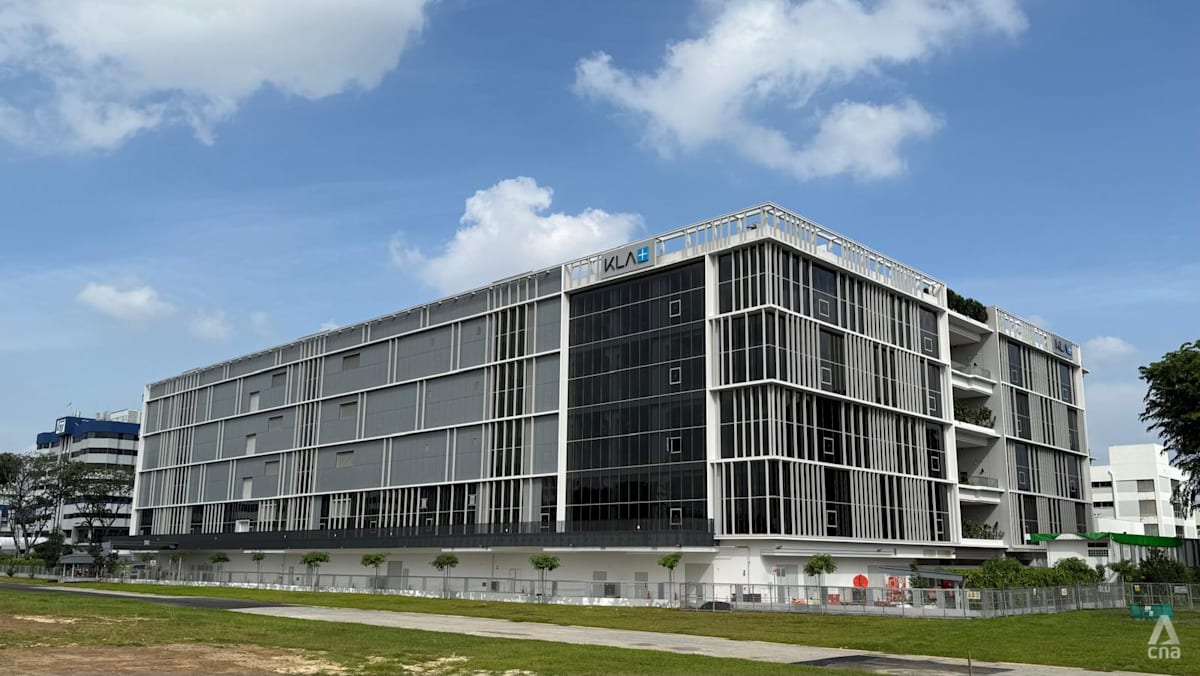
Semiconductor equipment manufacturer KLA Corporation launched an expansion at its Ang Mo Kio site on Nov 20, creating about 400 jobs.
The Bottom Line:
- KLA’s newly opened Building 22B spans 210,000 sq ft and accelerates production for advanced packaging, silicon photonics, and artificial intelligence applications.
- The combined footprint of Buildings 22A and 22B reaches approximately 420,000 sq ft, establishing Singapore as the company’s largest manufacturing site globally.
- An anticipated subsequent expansion phase could push total new job creation past 1,000 across research, supply chain, and manufacturing engineering roles.
The new 210,000 sq ft site enables the US-headquartered corporation to quicken production of its most advanced equipment for semiconductor manufacturing, according to a press release. Speaking at the launch ceremony, Deputy Prime Minister Gan Kim Yong said that Singapore accounts for about one-fifth of global semiconductor equipment output. Manufacturing chips requires precision equipment capable of measuring process variations and detecting defects early, he said.
“Singapore must keep building the specialised capabilities companies need to compete, and working with partners like KLA can support their growth while creating opportunities for its people,” Gan said at the launch.
Chief financial officer Bren Higgins said that this expansion increases the total size of KLA’s Ang Mo Kio facility to approximately 420,000 sq ft, positioning it as the firm’s primary manufacturing hub worldwide. The corporation currently employs more than 2,200 workers across multiple shifts in Singapore, Higgins noted.
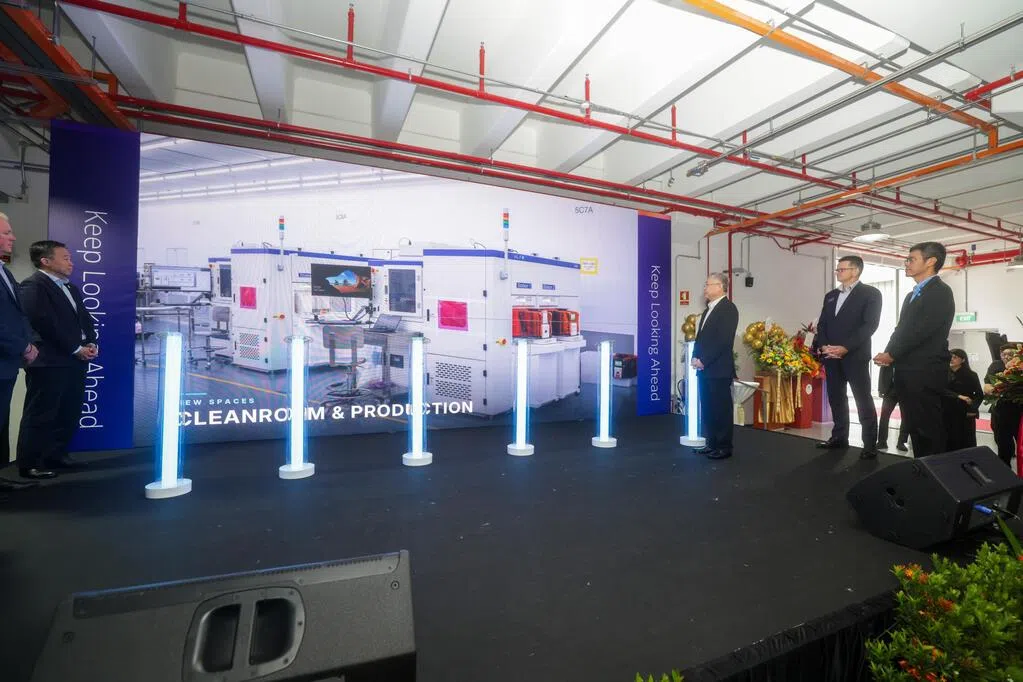
Manufacturing Footprint and Workforce Growth
Data from the Economic Development Board (EDB) indicates that the semiconductor sector accounts for nearly 6 per cent of Singapore’s gross domestic product, with a workforce exceeding 35,000 people. Building 22B alone creates at least 400 new jobs, spanning mechanical design engineering, materials evaluation, and product testing, Gan stated.
KLA Singapore country president and senior vice-president of global operations Theo Kneepkens outlined plans for another facility expansion, subject to relevant approvals. This next phase of growth will be bigger than the two current buildings combined and located nearby, Kneepkens added.
“Our plans for an additional phase reflect our conviction that Singapore, with its exceptional talent, supportive governance and strategic position, will remain indispensable to how the world manufactures critical semiconductor equipment that powers AI and advanced computing,” Kneepkens said.
Research Collaboration and Industry Outlook
The company’s Singapore site houses research and development, manufacturing, and corporate functions alongside one of its largest global technical training centres. During September, the Agency for Science, Technology and Research (A*STAR) revealed that it had entered into new or extended collaborative agreements with KLA, Applied Materials, and GlobalFoundries.
KLA will embark on a three-year collaboration with A*STAR’s Institute of Microelectronics to develop process control solutions for advanced packaging and silicon photonics technologies.
To support sector advances, Singapore committed S$800 million under Research Innovation and Enterprise 2030 (RIE 2030) to a semiconductor flagship programme aimed at strengthening research and innovation.
Kneepkens said that further expansion remains necessary to meet global manufacturing strategy requirements as final land arrangements proceed.
KLA Corporation traces its origins to 1975, when the company was founded as KLA Instruments with a focus on detecting photomask defects. In 1997, the organization reached a major turning point by merging with Tencor Instruments—a firm established in 1976 that pioneered laser-scanning technology for particle contamination detection—to create a unified source for semiconductor diagnostics.
Headquartered in Milpitas, California, the company now supplies process control and yield management systems used across all phases of wafer and integrated circuit production, from initial research and development to final volume manufacturing.
Disclaimer: The information provided in this article is for educational and market analysis purposes only and does not constitute financial, investment, or legal advice. Always consult with a certified financial professional before making investment decisions.
Related reading

FSU Swimming Sets Four Program Records at Georgia Invite
The Florida State University swimming and diving teams opened the Georgia Invite at the Gabrielsen Natatorium on Thursday...

I Interviewed 40 California Candidates; Most Couldn’t Answer Basic Questions
Over the past year, I interviewed roughly 40 candidates running for offices ranging from local city controller seats...

Martha’s Vineyard Ties Help Elect First Black Miss. Senator in 150 Years
In a recent column for the MV Times, West Tisbury resident Phyllis Segal details how grassroots efforts from...

Opinion: Lokken Argues Wisconsin Should Measure If Programs Meet Basic Needs
In an opinion piece published on Thursday by the Milwaukee Neighborhood News Service, Reed Lokken argues that the...