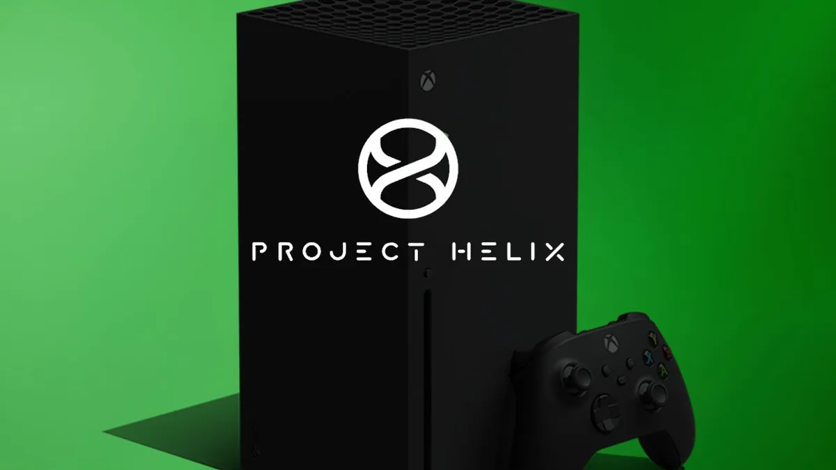
Hardware leaker KeplerL2 has revealed that next-generation graphics chips for the PlayStation 6 and Xbox Project Helix have reached tape-out, projecting a 56 TFLOPS compute capacity for Microsoft’s system and 40 TFLOPS for Sony’s upcoming console ahead of an anticipated late 2027 or 2028 release.
The race to define the next generation of console gaming has reached a critical manufacturing milestone. According to hardware tipster KeplerL2, the custom silicon chips designed for both Sony’s PlayStation 6 and Microsoft’s next-generation Xbox, internally designated as Project Helix, have officially taped out. This means the blueprinting phase is complete and the final layouts have been submitted to manufacturing facilities like TSMC.
Once a semiconductor reaches this stage, the architecture and core capabilities are effectively locked in. While the milestone brings the hardware closer to production, industry observers emphasize that raw specifications tell only part of the story as developers and manufacturers grapple with surging component expenses.
Compute Estimates Reveal a Theoretical Power Gap Between Helix and PlayStation 6
The leaked compute estimates point to a substantial numerical advantage for Microsoft’s next machine. The leaker claims 56 TFLOPS of processing capacity for the Xbox Helix, compared to 40 TFLOPS for the PlayStation 6. On paper, that gives the Xbox hardware roughly a 40 percent theoretical edge in raw graphical throughput.

To put those numbers into perspective, current-generation hardware operates at markedly lower thresholds. The base PlayStation 5 runs at 10.28 TFLOPS, the Xbox Series X reaches approximately 12 TFLOPS, and the mid-cycle PlayStation 5 Pro tops out at a typical 16.7 TFLOPS with an 18.05 TFLOPS peak. A 56 TFLOPS ceiling for Project Helix represents roughly triple the peak performance of the PS5 Pro on paper, though analysts caution that floating-point operations do not automatically translate to linear gains in real-world game frame rates.
Architectural Choices Separate Sony and Microsoft’s Silicon Strategies
Beneath the raw compute figures lie distinct engineering approaches for each system. Both consoles are expected to rely on the AMD Zen 6 CPU family and RDNA 5 graphics architecture, but their physical configurations diverge significantly.

Project Helix utilizes a chiplet design featuring a separate 144mm² System-on-Chip and a 264mm² GPU die, paired with a dedicated neural processing unit rated at up to 110 TOPS and a wider 192-bit memory bus. By contrast, the PlayStation 6 is reported to employ a monolithic design spanning roughly 280mm², integrating neural processing directly within the GPU and utilizing an estimated 30GB of GDDR7 memory across a 160-bit interface.
Escalating Memory Costs Threaten Four-Figure Retail Price Tags
While the hardware specifications highlight technical ambition, economic realities threaten to upend consumer expectations. Surging global demand for artificial intelligence infrastructure has severely restricted memory and storage supply, driving component costs upward across the consumer electronics market.
Production Timelines and Official Silence Keep Launch Windows Uncertain
Despite the advanced state of chip manufacturing, neither Sony, Microsoft, nor AMD has officially confirmed these specifications or established firm release dates. While chip production schedules point toward potential windows in late 2027 or 2028, corporate disclosures remain cautious.
Sony’s executive leadership recently admitted that the official launch timing for the PlayStation 6 remains undecided. Meanwhile, Microsoft has been consulting Xbox Insiders regarding foundational hardware decisions, including whether Project Helix should retain support for physical disc drives or feature exclusive software titles, leaving the market for next-generation gaming entirely unsettled.
Keep reading
AI Market Volatility Erases Trillions Before Rebound
Stock markets swung wildly over a recent two-week period, erasing and then recovering hundreds of billions of dollars...

Meta Unveils $1,299 VR Glasses With Lighter Design at Meta Connect
Meta unveiled its $1,299 Meta VR Glasses at the Connect conference on September 23, 2026, featuring a 100-gram...
TASK#STOMP Malware Uses Windows Tools to Steal Sensitive Enterprise Data
Security researchers have uncovered TASK#STOMP, a Windows backdoor using hidden PowerShell commands, VBScript installers, and scheduled tasks to...

South Korean Manufacturing Sentiment Rises on Chip and Cosmetic Exports
South Korea’s manufacturing sentiment rose for the fourth quarter as strong exports of semiconductors and cosmetics lifted the...